Photomasks used for integrated circuits manufacturing are commonly composed
of a chrome layer deposited on quartz or fused silica plates, which are
subsequently patterned for a photolithographic process. It is essential that the
chrome layer of the mask be defect free, with no obscure areas, no voids,
pinholes or scratches, so that there are no defects printed onto the photoresist
layer of the wafer in the photolithographic process, since defects in the chrome
layer of the photomask result in defects in the produced IC wafer.(1) Prompt
repair of these photomasks is crucial to keep a semiconductor fab running.
Ultrafast lasers allow to repair masks with feature sizes down to 0.15 µm and
the resulting high post-repair photomask transmission because of minimal mask
glass damage.
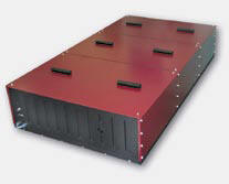
Del Mar Photonics, Inc. offers Teahupoo Rider amplified Ti:Sapphire laser for photomask repair applications.
|
|
Typical Specifications:
Teahupoo Rider
Amplified Femtosecond Ti:Sapphire Laser system
Fiber seed oscillator, regenerative amplifier, DPSS Nd:YAG pump laser
(10ns/532nm/1mJ), stretcher, compressor,
pulse picker, synchronization electronics, chiller and cover box.
Output: 0.1mJ@780nm, 2 kHz (fixed), 120fs
Specifications for seed femtosecond fiber laser:
Buccaneer with a SHG unit
Fiber laser with SH generation
Pulse Width (FWHM) < 120 fs
Wavelength 780+-10 nm (fixed)
Average output power >40 mW
Repetition rate 40 MHz
Spectral width ~ 7.5 nm
RF Out: SMA
Mode lock status: SMA
Polarization: vertical
Femtosecond micromachining brochure
Related Literature:
(1) Photomask Clear Defects Repair Using Ultrafast Laser Technology
(2) Material Processing Using Femtosecond Lasers: Repairing Patterned Photomasks
The use of ultrafast laser pulses is having an impact on materials processing in profound ways. “Machining” with femtosecond pulses affords considerable advantages over nanosecond pulses, such as subdiffraction-limited material ablation, where ablated spot dimensions are below that achievable when longer pulses are focused to the minimum spot size dictated by optical physics. These properties have been exploited to address what had become a critical problem in the semiconductor industry, the repair of patterned photomasks. We will describe how the fundamentals of femtosecond laser ablation have been implemented in a machine designed to repair photomasks. We will also describe experiments designed to deposit Cr metal onto fused-silica substrates using 100-fs, 400-nm light pulses at atmospheric pressure. Multiphoton dissociation of Cr(CO)6 adsorbed on fused-silica substrates initiates Cr deposition. The mechanisms for deposition on both transparent (fused silica) and absorbing (Cr metal) substrates are discussed. Finally, we describe experiments that were carried out to extend the photomask repair process to shorter wavelengths (below 200 nm) using light generated by frequency-mixing of ultrashort, 30-fs pulses in an Ar-filled capillary.
(3) Near-field optical
photomask repair with a femtosecond laser.
We present a high-resolution near-field optical tool designed for repair of
opaque defects in binary photomasks. Both instrument design and near-field
imaging and patterning results will be presented. Designed for ablative
processing of thin metal films, the MR-100 incorporates an industrial amplified
femtosecond laser, third harmonic generator and built-in autocorrelator. The
ultrashort duration of the femtosecond pulses enables the tool to remove chrome
layers with negligible damage to the surrounding metal or the underlying quartz
substrate. The micropipette based near-field writing head can deliver power
densities of hundreds of GW/cm2 to spots of several hundred nanometres and
below. Repairs on sample masks will be presented and the repair quality will be
discussed.