Del Mar Photonics - Newsletter - MCP products - How to choose MCP detector - Request a quote
Microchannel Plates and MCP Detectors and Imaging Systems
Microchannel Plates
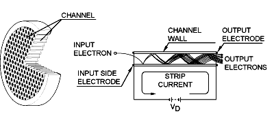
MCP is a specially fabricated plate that amplifies electron signal similar to secondary electron multiplier (SEM). Unlike SEM, MCP has several million independent channels and each channel works as independent electron multiplier. In other words, one can imagine MCP as an assembly of millions miniature SEMs. MCP consists of a two-dimensional periodic array of very-small diameter glass capillaries (channels) fused together and sliced in a thin plate. A single incident particle (ion, electron, photon etc.) enters a channel and emits an electron from the channel wall. Secondary electrons are accelerated by an electric field developed by a voltage applied across the both ends of the MCP. They travel along their parabolic trajectories until they in turn strike the channel surface, thus producing more secondary electrons. This process is repeated many times along the channel; as a result, this cascade process yields a cloud of several thousand electrons, which emerge from the rear of the plate. If two or more MCPs are operated in series, a single input event will generate a pulse of 108 or more electrons at the output.
Since the individual channels confine the pulse, the spatial pattern of electron pulses at the rear of the plate preserve the pattern (image) particles incident on the front surface. The output signals are typically collected in any of several ways, including metal or multimetal anodes, resistive anode (one- or two- dimensional), wedge and strip anode, Delay-Line Readout or on a phosphor screen deposited on a fiberoptic or other substrate.
Microchannel Plates have a combination of unique properties like high gain, high spatial resolution and high temporal resolution. They can be used in a large variety of applications including, imaging spectroscopy, electron spectroscopy and microscopy, mass spectrometry, astronomy, molecular and atomic collision studies, cluster physics etc. Most of these applications require only some of MCP properties, for example Time-of-Flight Mass Spectrometry require high temporal resolution of MCPs, imaging of single atoms in field ion microscopes or X-ray imaging of the Sun require mainly spatial resolution. Particle analyzers may be produced by using a MCP detector at the output of a electrostatic and/or magnetic dispersion system. Very high sensitivity optical, UV and EUV and X-ray spectrometers can also be produced with appropriate filtering and dispersive elements. The same microchannel plate technology is used to make visible light image intensifiers for night vision goggles and binoculars.
Detectors based on Microchannel Plates have variety of designs depending on the type of particles detected, throughput (counts/second), time and position resolution, imaging area, linearity and sensitivity, signal to noise ratio and other requirements. It's a challenge to detector developer to optimize detector design for particular application.
In general, each detector that uses MCPs consists of three parts:
1) A Converter - a mechanism to convert initial particles in photons or electrons,
2) An Assembly of MCPs - a mechanism to amplify initial single electron or photon event into electron pulse and
3) A Readout Device - a mechanism to detect the electron avalanche.
Del Mar Photonics supply Microchannel Plates, MCP assemblies as well as custom-made systems including mounting and readout device (s). This brochure describes Microchannel Plates, Open Microchannel Plates Detectors with Metal Anode and Open Imaging Detectors (Image Intensifiers).
Microchannel Plates
|
|
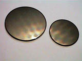
The microchannel plate is an open multiplier intended for registration of particles and radiations. MCPs represent 0.4-3.0 mm thick plates of round or rectangular shape. They have a honeycomb structure and contain in one square centimeter up to one million of separate channels of 5-15 m m diameter. In addition to design simplicity, small dimensions and absence of external voltage divider, MCPs feature high time and spatial resolution capability. |
| Model | Product Name+ | Buy Now |
| MCP 25-10E | Microchannel Plate MCP 25-10E |
|
| MCP 33-10E | Microchannel Plate MCP 33-10E |
|
| MCP 34-10 | Microchannel Plate MCP 34-10 |
|
| MCP 43-63 | Microchannel Plate MCP 43x63 |
|
| MCP 46-12 | Microchannel Plate MCP 46-12 |
|
| MCP 56-15 | Microchannel Plate MCP 56-15 |
|
| MCP 70-90 | Microchannel Plate MCP 70x90 |
|
Construction and Operation
A Microchannel Plate begins as a glass tube fitted with a solid, acid-etchable core and drawn via fiberoptic techniques to form single fibers. A number of these fibers are then stacked in a hexagonal array; the entire assembly is drawn again to form multi-fibers. The multi-fibers are then stacked together and fused at high temperature to form a boule.
The boule is sliced on a wafer saw to the required bias angle, edged to size, and then ground and polished to an optical finish. The individual slices are chemically processed to remove the solid core material, leaving a "honeycomb" structure of millions of tiny holes.
Through subsequent processing, this glass wafer is given its conductive and secondary emissive properties. Finally, a thin metal electrode (usually Inconel, Nichrome or chromium) is vacuum-deposited on both input and output surfaces of the wafer to electrically connect all the channels in parallel.
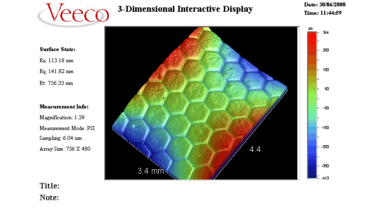 |
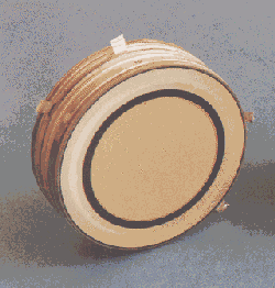
Honeycomb structure of Microchannel Plates. For additional images of Microchannel Plate surface at different spatial resolution click here. |
For normal operation, a bias of about 1000 Volts is applied across the microchannel plate, with the output at its most positive potential. The bias current flowing through the plate resistance is what supplies the electrons necessary to continue the secondary emission process. Electron multiplying process was described above. Below we consider most important properties of Microchannel Plates.
Shape and Size
Microchannel plate arrays may be fabricated in a wide variety of formats. The MCPs may range in size from 6mm to 100mm or larger, and they may be circular, rectangular, or virtually any other shape as required by the application or instrument geometry. In addition, a cylindrical or spherical radius of curvature may be provided to conform to the focal plane of an instrument.
A border glass area surrounds an effective area of MCP where channels are arrayed. Table below shows dimensions of standard MCPs, supplied by Del Mar Ventures.
| MCP type (part #) |
25-10E* |
33-10E |
34-10 |
46-12 |
56-15 |
43*63 |
70*90 |
| Diameter, mm
Length, mm Width, mm |
24.8 |
32.8 |
34 |
46 |
56 |
63 43 |
90 70 |
| Effective Diameter, mm |
18 |
25 |
30 |
40 |
50 |
38*58 |
65*85 |
| Channel Diameter, m m |
10 |
10 |
10 |
12 |
15 |
15 |
15 |
MCP Thickness and Channel Diameter
The length of the channel of a MCP is virtually its thickness. The ratio of the channel length (L) to the channel diameter (d) L/d, as well as the inherent secondary emission factor of the channel wall material determines the gain of the MCP. The standard MCPs are fabricated with a L/d ratio about 40 to 80.
Channel Bias Angle
The channel bias angle is an angle formed by the channel axis and the vertical axis to plate surface. Channels are tilted to prevent incident particles from passing through the channels. The optimum angle is between 5° and 15° .
Open Area Ratio (OAR)
The OAR is the ratio of the open area to the total effective area of the MCP. For hexagonal arrays OAR=(p *O 3/6)*(d/P)2 where d is a channel diameter and P is a pitch (period of the hexagonal structure, or c-c distance). For 10-12 structure (d=10m m, P=12m m) OAR=63%, for 12-15 it's 58%, for 15-18 it's 63%. OAR limits ultimate detection sensitivity of MCPs. Particles incident on the MCP between channels are not detected. In many applications it is desired to make OAR as large as possible for more efficient input of primary electrons. For this purpose, there are custom MCPs in which the glass channel walls on the input side have been etched to increase the OAR up to 70 to 80%.
Metal Coating (Electrodes)
Over the input and output surfaces of a MCP, Inconel, Ni-Cr or Cr is evaporated to form electrodes. The thickness of the electrodes is controlled to have a surface resistance of 100 to 200W between the MCP edge. In general, the electrodes are evaporated to uniformly penetrate into the channels. The penetration depth significantly affects the angular and energy distributions of the output electrons, and usually chosen to be in the range of the channel diameter multiplied by 0.5 to 2. In such demanding applications as image intensification where spatial resolution is of prime importance, the penetration depth of the electrodes is controlled to be deeper in order to collimate the output electrons.
Gain
The gain of an MCP, g, is given by the following equation using the length-to-diameter ratio of the channel: g= exp (G*(L/d), where G is the secondary emission characteristics of the channel called gain factor. This gain factor is an inherent characteristic of the channel wall material and represented by a function of the electric field intensity inside the channel. Generally, L/D is designed to be around 40, which produces a gain of 104 with an applied voltage of 1 kV.
When an even higher gain is required, two or three MCPs are used to configure the two-stage or three-stage MCP assembly. These stacked MCP detectors can offer higher gains up to 108-109. Multiple-stage MCP gains are not the simple multiplication of the gain of each MCP because of the gain saturation caused by space charge effect near the output region of channels.
In these configurations the spatial resolution is degraded to some extent because a multiplying electron current spreads into several channels as it enters the latter-stage MCP. On the other hand the saturation level increases by a factor equal to the number of those spread channels.
Pulse height distribution
When a single particle create a single electron event in MCP, the output pulse height distribution shows normally an exponential function. However, in the region where the gain is saturated due to space charge effect, the pulse height distribution becomes peaked. This phenomenon is observed in the MCPs operating at a high gain, for instance, stacked MCPs.
Pulse height distribution is usually characterized by the ratio of the half-width at peak (full width at half maximum: FWHM) to the peak value in the pulse height distribution: FWHM/A; it is normally expressed in percentage. In general, is shows 120% or less for two-stage MCPs and 80% or less for three-stage MCPs.
Transit time
The transit time of MCP assemblies is very small. Due to the shorter electron transit distance compared to the discrete dynode used in the conventional PMT or SEM, transit time of the electron avalanche in MCP channels is in 100 ps range. The width of the single event peak determined mainly by temporal characteristics of readout device and electronics. Ultimate time resolution can be achieved using anode configuration matched with 50 W connector cable.
Spatial Resolution
Since each channel of the MCP serves as an independent electron multiplier, the channel diameter and center-to-center (c-c) spacing determine MCP resolution. Channel diameters ranging from 5 m m (6 m m c-c) to 15 m m (18 m m c-c) are standard.
When the output from MCP is observed with a phosphor screen, the spatial resolution also depends on the MCP electrode depth penetrating into the channels, the space between the MCP and the phosphor screen, and the accelerating voltage. Typical spatial resolution of a MCP composed of 10 m m diameter channels, which is observed with a phosphor screen, is about 40 l/mm. In the stacked MCP, the spatial resolution is less compared to that of a single MCP because it spreads into many channels as it enters the latter-stage MCP, and also because the increased gain makes greater the electrostatic repulsion in the space when the electrons are released from the MCP.
Dark Current
A typical MCP shows an exceptionally low dark current, less than 0.5pA/cm2 at an applied voltage of 1 kV. Even with a two or three-stage MCP, the dark count rate is low, less than 3 cps/cm2 at an applied voltage of 1 kV per stage.
Resistance
Glass composition and reduction processing conditions (time and temperature) can control the MCP resistance. Considering the output saturation, a lower resistance is desirable; however, there is a limitation in lowering the resistance as the MCP operating temperature rises due to higher power consumption.
MCP resistance is typically in the range between 100 and 1000 MW . For applications requiring high output currents, low-resistance MCPs of 20 to 30 MW are available.
Microchannel Plate Detectors with Single Metal Anode (MCP-MA)
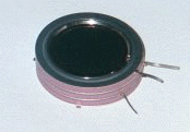 |
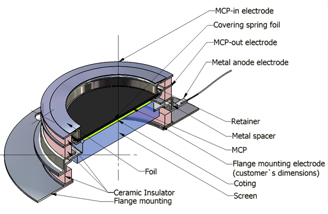
DEL MAR VENTURES Microchannel Plate Detectors MCP-MA series are an open MCP detectors with one or more microchannel plates and a single metal anode. They are intended for time-resolved detection and make use of high-speed response properties of the MCPs. MCP-MA detectors are used for photons and particles detection in vacuum chambers or in the space. |
|
The body of assembly is a metal-ceramic housing. Drawing shows two matched MCPs in V-stack (Chevron) assembly, which are fixed in place using retainer ring (above MCPs). Ceramic insulator rings are shown red. Detector is spot-welded to the support plate (available in different sizes). |
 |
All parts of the assembly are highest quality components. Metal parts are polished to avoid electric discharges. Two MCPs are connected to each other via thin (40 -50 mm) copper or stainless steel foil ring. Direction of channel bias angle in the first MCP is opposite to one in the second MCP (chevron assembly). Typical voltages necessary for a gain of 104, resistances and dark current densities of Microchannel Plates are shown in the table below. Each detector is supplied with individual MCP data.
Specifications:
|
MCP-MA25 |
MCP-MA34 |
MCP-MA46 |
|
| MCP detector body |
metal-ceramic housing |
||
| Effective area diameter, min |
18mm |
25mm |
40mm |
| MCP type | 25-5, 24-10, 25-10 etc. |
33-10 or 34-10 |
46-12 |
| MCP Diameter, mm |
24.2 or 24.8 |
32.8 or 34 |
46 |
| MCP Thickness, mm |
0.46 |
0.46 |
0.5 |
| MCP channels pore-pitch, mm |
5-6, or 10-12 |
10 -12 |
12-15 |
| Typical Gain, (one MCP) |
104 - 104 |
||
|
(2 stack) |
106 - 107 |
||
|
(3 stack) |
108 - 109 |
||
| Time resolution |
< 1ns |
||
| PHD (2 stack assembly) |
FWHM/A<120% |
||
| PHD (3 stack assembly) |
FWHM/A<80% |
||
| Output |
Single metal anode |
||
| Strip current |
<20mA |
||
Operation conditions:
Wiring Methods
In general, MCP assemblies can be operated with any electrode (MCP-in, MCP-out or anode) at a ground potential.
When applying a voltage, do not apply the necessary voltage to the MCP at once. Slowly increase the applied voltage, with maximum 100 V step, until the optimum rating is reached, and verify if the MCP operates properly. In this procedure, also check the dark current by connecting an ammeter to the readout device. If there is an increase in the dark current, which might result from a small discharge, immediately turn off the applied voltage. After some time (depending on the situation) has passed, apply voltage to the MCP again in the same manner as described above. Note that the applied voltage to the MCP should be increased as slowly as possible even after normal operation has been verified.
Recommended and maximum applied voltage to MCPs and readout devices are as follows:
Set this voltage according to the required gain, 700 -1000V per MCP typical, 1100 V maximum, MCP out at positive polarity.
This is normally set at about 100 - 200 V.
A system pressure better than 6.5*10-4 Pa (5 *10-6 Torr) is necessary for proper operation. The MCP detector has to be degassed before applying the maximum voltage. Because the MCP is operated with a high voltage of about 1 kV per stage, a relatively high degree of vacuum must be required. If the MCP is operated at a deficient vacuum, not only will the noise increase due to the ion generation in the channels, but also the lifetime may be shortened. In the worst case, the MCP may be damaged by discharge. Therefore, it is recommended that the MCP be operated at a degree of vacuum as high as possible. When using a new MCP, it is recommended that before applying a voltage to it, the system be evacuated at a pressure of 6.5*10-4 Pa (5*10-6 Torr) or below for more than 24 hours. If the evacuation time is short or the degree of vacuum is deficient, a discharge may occur.
MCP Detector Mounting
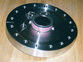
MCP-MA34 detector can be mounted on the standard vacuum flange or on any other substrate. It can be either spot-welded or connected with screws. Figure below shows MCP-MA34 mounted on the standard 6" ConFlat Flange.
Open Microchannel Plate Imaging Detectors (MCP-GPS and MCP-IFP)
 |
Open Microchannel Plate Imaging Detectors have a
design similar to MCP detectors with Metal Anode. Instead of simple metal
anode an aluminized phosphor screen is used as a readout device. An electron
cloud is drawn across a 0.7 mm gap by a high voltage onto micro-crystalline
phosphor screen where the kinetic energy of the electrons is released as
light. |
|
The phosphor screens deposited on a
glass window are realized in MCP-GPS series and on a fiber-optic plate in
MCP-IFP series. Drawing shows a cross-section of the imaging detector with a
fiber-optic plate.
The optical image can be viewed directly, or coupled to a camera. MCP-GPS and MCP-IFP imaging detectors are available in the same sizes and MCP-assembly options as MCP-MA detectors. Open imaging detectors must be operated in pressures of less than 6.5*10-4 Pa (5 *10-6 Torr). Recommended and maximum applied voltage to MCPs and phosphor screen are as follows:
Set this voltage according to the required gain, 700 -1000V per MCP typical, 1100 V maximum, MCP out at positive polarity.
A bias in the range 2.5-5 kV between MCP output and screen is required.
|
 |
Microchannel Plate detectors optimized for imaging VUV and EUV
radiation
Next generation lithography research is one of the potential applications of the
new Microchannel Plate detectors optimized for imaging VUV and EUV radiation.
Current advanced lithographic equipment employs excimer lasers to produce
feature sizes at 180 nm. Extreme ultraviolet (EUV) lithography tools will use
13.5 nm light to image chips with feature sizes below 45 nm. Much development
work is still required in EUV radiation sources. Del Mar Ventures provide a
complete program of stationary and gated MCP- Detectors for the registration of
X-ray- and UV-radiation below 2000 Å. Each equipped with a single Au coated MCP
plate and a phosphor screen on a fiber optic plate, which also serves as a
vacuum to air interface. Devending on the detector model phosphor screen is
either uniform or sectioned in several independent sectors or stripes. In
multi-frame units, each individual sector or stripe can be gated separately with
a time resolusion as short as 3 ns. This allows to obtain images or spectra or
both at individual times. Gated MCP detectors supplied with optional high
voltage pulse generator that provides four high voltage outputs with variable
delay time and width. Versatile trigger options, including an internal delay
generator allow for an easy adaptation to the experimental requirements.
Microchannel Plate Detectors MCP-MA
DEL MAR Microchannel Plate Detectors MCP-MA series are an open MCP detectors
with one or more microchannel plates and a single metal anode. They are intended
for time-resolved detection and make use of high-speed response properties of
the MCPs. MCP-MA detectors are designed for photons and particles detection in
vacuum chambers or in the space.
MCP-MA detectors are used in a variety of applications including UV, VUV and EUV
spectroscopy, atomic and molecular physics, TOF mass–spectrometry of clusters
and biomolecules, surface studies and space research.
MCP-MA detectors supplied as a totally assembled unit that can be easily mounted
on any support substrate or directly on a vacuum flange. They also can be
supplied premounted on a standard ConFlat flanges.
| Model | Product Name+ | Buy Now |
| MCP 34/2 G | Microchannel plate detector MCP 34/2 G |
|
| MCP-MA 25/2 | Microchannel plate detector MCP-MA 25/2 |
|
| MCP-MA 25/2 SP37 | Microchannel plate detector MCP-MA 25/2 |
|
| MCP-MA 25/2 SP70 | Microchannel plate detector MCP-MA 25/2 |
|
| MCP-GPS 34/2 | Microchannel plate imaging detector MCP-GPS 34/2 |
|
| MCP-IFP 25/2 | Microchannel plate imaging detector MCP-IFP 25/2 |
|
| MCP-IFP 34/2 | Microchannel plate imaging detector MCP-IFP 34/2 |
|
| Displaying 1 to 7 (of 7 products) |
![]()
References below are now reviewed by MCP Project Leader.
References:
1 - 2 -
3 - 4 -
5 - 6 -
7 - 8 -
9 - 10 -
11 - 12 -
13 - 14 -
15 - 16 -
17 - 18 - 19 -
20 - 21 -
22 - 23 -
24 - 25 -
26 - 27 -
28 -
29 - 30
31 - 32 -
33
more:
Microchannel plate response to high-intensity ion bunches.
(pdf)
Nuclear Instruments and Methods in Physics Research Section A: Accelerators,
Spectrometers, Detectors and Associated Equipment, Volume 557, Issue 2, Pages
516-522
S. Coeck, M. Beck, B. Delauré, V. Golovko, M. Herbane, A. Lindroth, S. Kopecky,
V. Kozlov, I. Kraev, T. Phalet
High-resolution ion time-of-flight analysis for measuring
molecular velocity distributions (abstract)
Y. Kim, S. Ansari, B. Zwickl, and H. Meyer
Department of Physics and Astronomy, The University of Georgia, Athens, Georgia
30602-2451
Molecular beam scattering of NO + Ne: A joint theoretical and
experimental study (abstract)
Y. Kim and H. Meyer
Department of Physics and Astronomy, The University of Georgia, Athens, Georgia
30602-2451
M. H. Alexander
Department of Chemistry and Biochemistry, The University of Maryland, College
Park, Maryland 20742-2021
A comparison between ion-to-photon and microchannel plate detectors
F. Dubois, R. Knochenmuss, R. Zenobi, A. Brunelle, C. Deprun, Y. Le Beyec
Rapid Communications in Mass Spectrometry
Volume: 13, Issue: 9, Date: 15 May 1999, Pages: 786-791
Using a superconducting tunnel junction detector to measure the secondary
electron emission efficiency for a microchannel plate detector bombarded by
large molecular ions
G. Westmacott, M. Frank, S. E. Labov, W. H. Benner
Rapid Communications in Mass Spectrometry
Volume: 14, Issue: 19, Date: 15 October 2000, Pages: 1854-1861
Optimization of an ion-to-photon detector for large molecules in mass
spectrometry
F. Dubois, R. Knochenmuss, R. Zenobi
Rapid Communications in Mass Spectrometry
Volume: 13, Issue: 19, Date: 15 October 1999, Pages: 1958-1967
Relation between breakdown voltage and prebreakdown current in vacuum gap
Eiji Takahashi, Akinori Ebe, Kiyoshi Ogata, Yoshinori Hayashi, Daisuke Makabe,
Mototaka Sone
Electrical Engineering in Japan
Volume: 131, Issue: 4, Date: June 2000, Pages: 11-18
Energy-sensitive cryogenic detectors for high-mass biomolecule mass spectrometry
Matthias Frank, Simon E. Labov, Garrett Westmacott, W. Henry Benner
Mass Spectrometry Reviews
Volume: 18, Issue: 3-4, Date: 1999, Pages: 155-186
Rapid, high-sensitivity imaging of radiolabeled gels with microchannel plate
detectors
John E. Lees, Paul G. Richards
Electrophoresis
Volume: 20, Issue: 10, Date: No. 10 July 1999, Pages: 2139-2143
Journal of Mass Spectrometry
Volume: 36, Issue: 4, Date: April 2001, Pages: 446-457
Abstract PDF Full Text (Size: 117K) Score: 0.77
Journal of Mass Spectrometry
Volume: 36, Issue: 1, Date: January 2001, Pages: 107-118
Miniature time-of-flight mass spectrometer using a flexible circuitboard
reflector
Timothy J. Cornish, Scott Ecelberger, Will Brinckerhoff
Rapid Communications in Mass Spectrometry
Volume: 14, Issue: 24, Date: , Pages: 2408-2411
Investigating ion-surface collisions with a niobium superconducting tunnel
junction detector in a time-of-flight mass spectrometer
G. Westmacott, F. Zhong, M. Frank, S. Friedrich, S. E. Labov, W. H. Benner
Rapid Communications in Mass Spectrometry
Volume: 14, Issue: 7, Date: 15 April 2000, Pages: 600-607
A novel scheme for the time-of-flight analysis of extended ion packets
Eugene Moskovets, Akos Vertes
Rapid Communications in Mass Spectrometry
Volume: 13, Issue: 22, Date: 30 November 1999, Pages: 2244-2248
High-efficiency Detection of 66 000 Da Protein Molecules Using a Cryogenic
Detector in a Matrix-assisted Laser Desorption/Ionization Time-of-flight Mass
Spectrometer
M. Frank, C. A. Mears, Simon E. Labov, W. H. Benner, D. Horn, J. M. Jaklevic, A.
T. Barfknecht
Rapid Communications in Mass Spectrometry
Volume: 10, Issue: 15, Date: December 1996, Pages: 1946-1950
Temporal and spatial resolution of scattered and recoiled atoms for surface
elemental and structural analysis
J. W. Rabalais
Surface and Interface Analysis
Volume: 27, Issue: 4, Date: April 1999, Pages: 171-178
Imaging x-ray fluorescence spectroscopy using microchannel plate relay optics
A. P. Martin, A. N. Brunton, G. W. Fraser, A. D. Holland, A. Keay, J. Hill, N.
Nelms, I. C. E. Turcu, R. Allott, N. Lisi, N. Spencer
X-Ray Spectrometry
Volume: 28, Issue: 1, Date: January/February 1999, Pages: 64-70
Application of the post-source pulse-focusing technique in matrix-assisted laser
desorption/ionization time-of-flight mass spectrometry: optimization of the
experimental parameters and their influence on the capability of the method
Matthias Amft, Friedrich Moritz, Christian Weickhardt, Jьrgen Grotemeyer
Rapid Communications in Mass Spectrometry
Volume: 12, Issue: 23, Date: 15 December 1998, Pages: 1879-1888
Fundamentals of Focal Plane Detectors
Keith Birkinshaw
Journal of Mass Spectrometry
Volume: 32, Issue: 8, Date: August 1997, Pages: 795-806
A comparison between ion-to-photon and microchannel plate detectors
F. Dubois 1, R. Knochenmuss 1, R. Zenobi 1 *, A. Brunelle 2, C. Deprun 2, Y. Le
Beyec 2
1Laboratorium für Organische Chemie, ETHZ, 8092 Zürich, Switzerland
2Institut de Physique Nucléaire, CNRS-IN2P3, 91406 Orsay Cedex, France
*Correspondence to R. Zenobi, Laboratorium für Organische Chemie, ETHZ, 8092
Zürich, Switzerland
Funded by:
Kommission für Technologie und Innovation; Grant Number: 3165.1
Bundesamt für Bildung und Wissenschaft; Grant Number: COST D5
An alternative detector for time-of-flight mass spectrometry, the ion-to-photon
detector, detecting light produced when ions impact a surface coated with a
fluorescent compound, was compared to a conventional microchannel plate
detector. Single ion experiments showed that, for a given energy, the efficiency
of the ion-to-photon detector relative to the microchannel plate detector
decreases as the molecular mass of the impinging ion increases. This decrease
becomes less pronounced for larger ions. Seen as a function of the ion velocity,
a linear relationship was found. The conversions into photons and electrons were
also compared. It was found that 22 keV ions up to 150 Da produced more photons
than secondary electrons. For larger ions at this energy, the opposite was
observed.
Using a superconducting tunnel junction detector to measure the secondary
electron emission efficiency for a microchannel plate detector bombarded by
large molecular ions
G. Westmacott 1, M. Frank 2, S. E. Labov 2, W. H. Benner 1 *
1Lawrence Berkeley National Laboratory, 1 Cyclotron Road, Berkeley, CA 94720,
USA
2Lawrence Livermore National Laboratory, 7000 East Ave., Livermore, CA 94551,
USA
*Correspondence to W. H. Benner, Lawrence Berkeley National Laborato 1 Cyclotron
Road, Berkeley, CA 94720, USA
Funded by:
US Department of Energy; Grant Number: DE-AC03-76SF00098, W-7405-ENG-48
An energy-sensitive superconducting tunnel junction (STJ) detector was used to
measure the secondary electron emission efficiency, e, for a microchannel plate
(MCP) detector bombarded by large (up to 66 kDa), slow moving (<40 km/s)
molecular ions. The method used is new and provides a more direct procedure for
measuring the efficiency of secondary electron emission from a surface. Both
detectors were exposed simultaneously to nearly identical ion fluxes. By
exposing only a small area of the MCP detector to ions, such that the area
exposed was effectively the same as the size of the STJ detector, the number of
ions detected with each detector were directly comparable. The STJ detector is
100% efficient for detecting ions in the energy regime investigated and
therefore it can be used to measure the detection efficiency and secondary
electron emission efficiency of the MCP. The results are consistent with
measurements made by other groups and provide further characterization of the
loss in sensitivity noted previously when MCP detectors have been used to detect
high-mass ions. Individual molecular ions of mass 66 kDa with 30 keV kinetic
energy were measured to have about a 5% probability of producing one or more
electrons when impacting the MCP. When ion energy was reduced to 10 keV, the
detection probability decreased to 1 %. The secondary electron yield was
calculated from the secondary electron emission efficiency and found to scale
linearly with the mass of the impinging molecular ion and to about the fourth
power of ion velocity. Secondary electrons were observed for primary ion impacts
>5 km/s, regardless of mass, and no evidence of a velocity (detection) threshold
was observed.
Optimization of an ion-to-photon detector for large molecules in mass
spectrometry
F. Dubois, R. Knochenmuss, R. Zenobi *
Department of Chemistry, Swiss Federal Institute of Technology (ETH), 8092
Zürich, Switzerland
*Correspondence to R. Zenobi, Department of Chemistry, ETH, 8092 Zürich,
Switzerland
Funded by:
Kommission für Technologie and Innovation; Grant Number: 3165.1
Ion packets can be detected in time-of-flight mass spectrometry by collecting
the photons that are produced during the impact of the packets with a
scintillator. The photon yield is a function of the ion energy. It was found
that post-acceleration of the particles in front of the scintillator was an
efficient way of increasing signal intensities. For the same total ion energy,
the intensities were larger with post-acceleration than when only increasing the
initial ion kinetic energy. A venetian blind dynode, converting the primary ion
beam into electrons/secondary ions, was also introduced. Positive or negative
secondary particles produced on the dynode surface could be accelerated to the
scintillator. Electrons were found to give the highest signals. Intensities
similar to those measured with microchannel plates were found. The linearity and
onset of saturation of the microchannel plates and the ion-to-photon detector
were compared. At optimum operating conditions, the ion-to-photon detector gave
around 10 times higher signals than the microchannel plates for heavy ions (150
kDa), with similar mass resolution.
Energy-sensitive cryogenic detectors for high-mass biomolecule mass
spectrometry*
Matthias Frank 1 *, Simon E. Labov 1, Garrett Westmacott 2, W. Henry Benner 2
1Lawrence Livermore National Laboratory, Physics Directorate, V-Division,
Livermore, CA 94551
2Lawrence Berkeley National Laboratory, Human Genome Center Instrumentation
Group, 1 Cyclotron Rd., Berkeley, CA 94720
*Correspondence to Matthias Frank, Lawrence Livermore National Laboratory, P.O.
Box 808, Mail Stop L-418, Livermore, CA 94551
**This article is a US Government work and, as such, is in the public domain in
the United States of America.
Keywords
cryogenic detectors; calorimetric detectors; high-mass detectors; time-of-flight
mass spectrometry
Energy-sensitive calorimetric detectors that operate at low temperatures (
cryogenic detectors ) have recently been applied for the first time as ion
detectors in time-of-flight mass spectrometry. Compared to conventional,
ionization-based detectors, which rely on secondary electron formation or the
charge created in a semiconductor, cryogenic detectors measure low-energy solid
state excitations created by a particle impact. This energy sensitivity of
cryogenic detectors results in several potential advantages for TOF-MS.
Cryogenic detectors are expected to have near 100% efficiency even for very
large, slow-moving molecules, in contrast to microchannel plates whose
efficiency drops considerably at large mass. Thus, cryogenic detectors could
contribute to extending the mass range accessible by TOF-MS and help improving
detection limits. In addition, the energy resolution provided by cryogenic
detectors can be used for charge discrimination and studies of ion
fragmentation, ion-detector interaction, and internal energies of large
molecular ions. Cryogenic detectors could therefore prove to be a valuable
diagnostic tool in TOF-MS. Here, we give a general introduction to the cryogenic
detector types most applicable to TOF-MS including those types already used in
several TOF-MS experiments. We review and compare the results of these
experiments, discuss practical aspects of operating cryogenic detectors in
TOF-MS systems, and describe potential near future improvements of cryogenic
detectors for applications in mass spectrometry.
Rapid, high-sensitivity imaging of radiolabeled gels with microchannel plate
detectors
John E. Lees 1 *, Paul G. Richards 2
1Space Research Centre, University of Leicester, Leicester, UK
2MRC Toxicology Unit, Leicester, UK
email: John E. Lees (leeqstar.le.ac.uk)
Keywords
Two-dimensional gel electrophoresis; Tritium; Imaging; Microchannel plates;
Organophosphates
A michrochannel plate detector has been used to image tritium-labeled protein on
one- and two-dimensional electrophoresis gels. The good spatial resolution (70
microns) and high sensitivity (6.0 dpm/mm2) of the imaging system allows
detection of low levels (femto moles) of labelled proteins. We are currently
using the detector for identification of new targets involved in organophosphate
neurotoxicity.
Miniature time-of-flight mass spectrometer using a flexible circuitboard
reflector
Timothy J. Cornish *, Scott Ecelberger, Will Brinckerhoff
Johns Hopkins University Applied Physics Laboratory, 11100 Johns Hopkins Road,
Laurel, MD 20723, USA
*Correspondence to Timothy J. Cornish, Johns Hopkins University Applied Physics
Laboratory, 11100 Johns Hopkins Road, Laurel, MD 20723 USA
An innovative design for a miniature time-of-flight mass spectrometer has been
developed employing several newly designed components. These include: (1) a
gridless, focusing ion source allowing for the use of very high extraction
energies in a maintenance-free design, (2) a new method of construction for an
ion reflector using rolled flexible circuitboard material, and (3) an improved
center-hole microchannel plate detector assembly that significantly reduces the
noise (or ringing ) inherent in the coaxial design. A prototype time-of-flight
instrument was constructed and used to evaluate the performance of these
components. Compared to previous designs, results indicate that background noise
for data acquired on this instrument is substantially reduced, resolution is
improved, and the potential for mass producing this instrument in an inexpensive
and rugged package for field-portable and remote installations is significantly
enhanced.
Investigating ion-surface collisions with a niobium superconducting tunnel
junction detector in a time-of-flight mass spectrometer
G. Westmacott 1, F. Zhong 1, M. Frank 2, S. Friedrich 2, S. E. Labov 2, W. H.
Benner 1 *
1Lawrence Berkeley National Laboratory, MS 70A-3363, 1 Cyclotron Road, Berkeley,
CA 94720, USA
2Lawrence Livermore National Laboratory, 7000 East Ave., L-418 Livermore, CA
94551, USA
*Correspondence to W. H. Benner, Lawrence Berkeley National Laboratory MS
70A-3363, 1 Cyclotron Road, Berkeley, CA 94720, USA
Funded by:
US Department of Energy; Grant Number: DE-AC03-76SF00098, W-7405-ENG-48
The performance of an energy sensitive, niobium superconducting tunnel junction
(STJ) detector is investigated by measuring the pulse height produced by
impacting molecular and atomic ions at different kinetic energies. Ions are
produced by laser desorption and matrix-assisted laser desorption in a
time-of-flight mass spectrometer. Our results show that the STJ detector pulse
height decreases for increasing molecular ion mass, passes through a minimum at
around 2000 Da, and then increases with increasing mass of molecular ions above
2000 Da. The detector does not show a decline in sensitivity for high mass ions
as is observed with microchannel plate ion detectors. These detector plus height
measurements are discussed in terms of several physical mechanisms involved in
an ion-surface collision.
A novel scheme for the time-of-flight analysis of extended ion packets
Eugene Moskovets, Akos Vertes *
Department of Chemistry, The George Washington University, Washington, DC 20052,
USA
email: Akos Vertes (vertes@gwu.edu)
*Correspondence to Akos Vertes, Department of Chemistry, The George Washington
University, Washington, DC 20052, USA
A new scheme is proposed for providing enhanced time-of-flight focusing of
spatially extended ion packets moving with close to uniform velocity,
sufficiently high for reliable ion detection. The arrangement consists of two
decelerating regions with homogeneous electric fields similar to the two-stage
ion reflector. The decelerating field in the first decelerating stage is created
in a pulsed fashion after the ion packet has entered the first region. The
effect of fringe fields produced by shielding rings and the microchannel plate
detector is discussed.
High-efficiency Detection of 66 000 Da Protein Molecules Using a Cryogenic
Detector in a Matrix-assisted Laser Desorption/Ionization Time-of-flight Mass
Spectrometer
M. Frank 1 *, C. A. Mears 1, Simon E. Labov 1, W. H. Benner 2, D. Horn 2, J. M.
Jaklevic 2, A. T. Barfknecht 3
1Lawrence Livermore National Laboratory, Physics & Space Technology, V-Division,
Livermore, CA 94551 USA
2Lawrence Berkeley National Laboratory, Human Genome Center Instrumentation
Group, 1 Cyclotron Rd., Berkeley, CA 94720, USA
3Conductus, Inc., Sunnyvale, CA, USA
We present the first experimental results obtained using a cryogenically-cooled
Nb-Al2O3-Nb superconductor-insulator-superconductor (SIS) tunnel junction
detector operating at 1.3 K as an ion detector in a time-of-flight mass
spectrometer. As opposed to microchannel-plate ion detectors (MCPs) commonly
used in such systems, cryogenic detectors such as SIS detectors offer a near
100% detection efficiency for all ions including single, very massive,
slow-moving macromolecules. We describe the operating principle of an SIS
detector and its use as an ion detector in our matrix-assisted laser desorption/ionization
(MALDI) time-of-flight mass spectrometer and compare its response to an MCP
detector operated in the same system. To our knowledge, this is the first direct
comparison of these detector types in this application. A comparison of count
rates and time-of-flight spectra obtained with both detectors for human serum
albumin (molecular weight 66 000 Da) indicates a two to three orders of
magnitude higher detection efficiency per unit area for the SIS detector at this
mass. For higher molecular masses we expect an even higher relative efficiency
for cryogenic detectors since MCPs show a rapid decline in detection efficiency
as ion mass increases, which is not expected to be the case for cryogenic
detectors. Our results imply that time-of-flight techniques could be extended
beyond the current upper mass limit if cryogenic detectors are used. Initially,
cryogenic detectors will be used for the analysis of large protein molecules. If
non-fragmenting ionization techniques can be perfected, cryogenic detectors will
also open the possibility of the rapid analysis of large DNA molecules and
perhaps intact microorganisms.
*Correspondence to M. Frank, Lawrence Livermore National Laboratory, Physics &
Space Technology, V-Division, Livermore, CA 94551 USA
Funding Agency: US Department of Energy; Grant Number: W-7405-ENG-48
Funding Agency: Office of Energy Research, Office of Health and Envirnomental
Research, Human Gerome Project, US Department of Energy; Grant Number:
DE-AC03-76SF00098
Temporal and spatial resolution of scattered and recoiled atoms for surface
elemental and structural analysis
J. W. Rabalais *
Department of Chemistry, University of Houston, Houston, TX 77204-5641, USA
Keywords
ion scattering; time of flight; surface analysis; surface structure
Developments in low-energy ion scattering over the past 10 years have led to new
techniques for surface elemental and structural analyses. The fundamental
physics involved in these new methods is summarized herein and some examples of
the applications of the techniques are presented. Three major new developments
are considered. First, time-of-flight scattering and recoiling spectrometry (ToF-SARS)
takes advantage of ToF techniques to detect simultaneously both ions and fast
neutrals that are scattered and recoiled from surfaces. Elemental analyses are
obtained by application of binary collision theory, and structural analyses are
performed by rotation of the sample in order to measure intensity changes as a
function of incident and azimuthal angles. Second, scattering and recoiling
imaging spectrometry (SARIS) takes advantage of a large position-sensitive
microchannel plate detector, coupled with ToF techniques, to capture
element-specific, time-resolved, spatial and intensity distributions of
scattered and recoiled atoms from surfaces. These images combine atomic scale
microscopy and spatial averaging because they are created from a macroscopic
surface area but they are directly related to the atomic arrangement of the
surface at the subnanoscale level; the features of the images are sensitive to
changes in interatomic spacings at a level of <0.1 Å. Third, a classical ion
trajectory simulation program, called scattering and recoiling imaging code (SARIC),
which is designed specifically for structural interpretation of ToF-SARS and
SARIS data, has been developed. This program allows quantitative comparison of
experimental and simulated data for surface structure determinations.
*Correspondence to J. W. Rabalais, Department of Chemistry, University of
Houston, Houston, TX 77204-5641, USA
Funding Agency: National Science Foundation; Grant Number: CHE-970066S
Funding Agency: R. A. Welch Foundation; Grant Number: E-656
References
1 . C. Kim, C. Höfner, V. Bykov and J. W. Rabalais, Nucl. Instrum. Methods Phys.
Res. B 125, 315 (1997).
2 . J. W. Rabalais, Science 250, 521 (1990); CRC Crit. Rev. Solid State Mater
Sci. 14, 319 (1988).
3 . O. Grizzi, M. Shi, H. Bu and J. W. Rabalais, Rev. Sci. Instrum. 61, 740
(1990).
4 . C. Kim, C. Höfner, A. H. Al-Bayati and J. W. Rabalais, Rev. Sci. Instrum.
69, 1676 (1998); C. Kim, A. Al-Bayati and J. W. Rabalais, Rev. Sci. Instrum. 69,
1289 (1998); J. Yao, C. Kim and J. W. Rabalais, Rev. Sci. Instrum. 69, 306
(1998).
5 . E. S. Parilis, L. M. Kishinevsky, N. Yu. Turaev, B. E. Baklitzky, F. F.
Umarov, V. Kh. Verleger and I. S. Bitensky, Atomic Collisions on Solids.
North-Holland, New York (1993).
6 . E. S. Mashkova and V. A. Molchanov, Medium-Energy Ion Reflection From
Solids. North-Holland, Amsterdam (1985).
7 . M. T. Robinson, in Sputtering by Particle Bombardment, edited by R. Behrish,
p. 74. Springer, Berlin (1981).
8 . J. F. Ziegler, J. P. Biersack and U. Littmark, in The Stopping and Range of
Ions in Solids, edited by J. F. Ziegler. Pergamon Press, New York (1985).
9 . V. Bykov, C. Kim, M. M. Sung, K. J. Boyd, S. S. Todorov and J. W. Rabalais,
Nucl. Instrum. Methods Phys. Res. B 114, 371 (1996).
10 . M. M. Sung, V. Bykov, A. Al-Bayati, C. Kim, S. S. Todorov and J. W.
Rabalais, Scanning Microsc. 9, 321 (1995).
11 . M. T. Robinson and O. S. Oen, Appl. Phys. Lett. 2, 30 (1963); J. Lindhard,
K. Dan. Vidensk. Selsk. Mat. Fys. Medd. 34, 1 (1965); D. V. Morgan (ed),
Channeling, Theory, Observation and Applications, Wiley, Chichester (1973).
12 . J. Ahn and J. W. Rabalais, J. Phys. Chem. B 102, 223 (1998).
13 . A. Niehof and W. Heiland, Nucl. Instrum. Methods B 48, 306 (1990).
14 . R. S. Williams and J. A. Yarmoff, Nucl. Instrum. Methods 218, 235 (1983);
J. A. Yarmoff, R. Blumentahl and R. S. Williams, Surf. Sci. 165, 1 (1986).
15 . O. Grizzi, M. Shi, H. Bu, J. W. Rabalais and P. Hochmann, Phys. Rev. B 40,
10147 (1989).
16 . E. Vlieg, I. K. Robinson and K. Kern, Surf. Sci. 233, 248 (1990); S.
Speller, J. Bömermann, S. Molitor, T. Rauch and W. Heiland, Surf. Sci. 331, 1070
(1995); A. Niehof and W. Heiland, Nucl. Instrum. Methods Phys. Res. B 48, 306
(1990); M. Guillope and B. Legrand, Surf. Sci. 215, 577 (1989); M. Garofalo, E.
Tosatti and F. Ercolessi, Surf. Sci. 188, 321 (1987); H. Derks, J. Möller and W.
Heiland, Surf. Sci. Nucl. Instrum. Methods Phys. Res. B 188, L685 (1987); H.
Derks, H. Hemme, W. Heiland and S. H. Overbury, 23, 374 (1987); K.-M. Ho and K.
P. Bohnen, Phys. Rev. Lett. 59, 1833 (1987); M. Copel and T. Gustafsson, Phys.
Rev. Lett. 57, 723 (1986).
17 . J. Lindhard, Nath. Fys. Medd. 34, no. 14 (1965).
18 . C. Hofner and J. W. Rabalais, Surf. Sci. 400, 189 (1997).
19 . C. Hofner, B. Bykov and J. W. Rabalais, Surf. Sci. 393, 184 (1997).
20 . C. Kim, C. Hofner and J. W. Rabalais, Surf. Sci. 388, L1058 (1997).
21 . N. Materer, U. Starke, A. Barbieri, R. Doll, K. Heinz, M. A. Van Hove and
G. A. Somorjai, Surf. Sci. 325, 207 (1995); K. Hayek, H. Glassl, A. Gutmann, H.
Leonhard, M. Prutton, S. P. Tear and M. R. Welton-Cook, Surf. Sci. 152, 419
(1985); R. Feder, H. Pleyer, P. Bauer and N. Mueller, Surf. Sci. 109, 419
(1981); D. L. Adams, H. B. Nielsen and M. A. Van Hove, Phys. Rev. B 20, 4789
(1979); M. A. Van Hove, W. H. Weinberg and C.-M. Chan, Low Energy Electron
Diffraction. Springer, Berlin (1986).
22 . J. A. Davies, D. P. Jackson, P. R. Norton, D. E. Posner and W. N. Unertl,
Solid State Commun. 34, 41 (1980); J. F. van der Veen, R. G. Smeenk, R. M. Tromp
and F. W. Saris, Surf. Sci. 79, 219 (1979).
23 . P. J. Feibelman, Surf. Sci. 360, 297 (1966).
Imaging x-ray fluorescence spectroscopy using microchannel plate relay optics
A. P. Martin 1, A. N. Brunton 1, G. W. Fraser 1 *, A. D. Holland 1, A. Keay 1,
J. Hill 1, N. Nelms 1, I. C. E. Turcu 2, R. Allott 2, N. Lisi 2, N. Spencer 2
1X-ray Astronomy Group, Department of Physics and Astronomy, University of
Leicester, University Road, Leicester, Leicestershire LE1 7RH, UK
2Lasers for Science Facility, Rutherford Appleton Laboratory, Chilton, Didcot,
Oxfordshire OX11 0QX, UK
email: G. W. Fraser (gwf@star.le.ac.uk)
*Correspondence to G. W. Fraser, X-ray Astronomy Group, Department of Physics
and Astronomy, University of Leicester, University Road, Leicester,
Leicestershire LE1 7RH, UK
Funded by:
UK PPARC
A novel imaging low-energy x-ray fluorescence spectrometer with no moving parts,
based on a microchannel plate relay optic and an open electrode charge-coupled
device with good sub-keV quantum efficiency, is described. Results from a proof
of principle experiment using the Rutherford Appleton Laboratory picosecond
pulsed laser plasma x-ray source are described and the performance limits of the
spectrometer explored.
Application of the post-source pulse-focusing technique in matrix-assisted laser
desorption/ionization time-of-flight mass spectrometry: optimization of the
experimental parameters and their influence on the capability of the method
Matthias Amft, Friedrich Moritz, Christian Weickhardt *, Jürgen Grotemeyer
Lehrstuhl für Physikalische Chemie und Analytik, Brandenburgische Technische
Universität Cottbus, Am Technologiepark 1, D-03099 Kolkwitz, Germany
Keywords
Company LSI Laser Science Inc., Newton, MA; Product nitrogen laser system;
Company El-mul Technologies, Yavne, Israel; Product microsphere plate
This paper describes experiments demonstrating the performance of a linear
time-of-flight mass spectrometer equipped with the post-source pulse-focusing (PSPF)
technique. The influence of various experimental parameters like the shape of
the PSPF pulse on the performance of the instrument is discussed. The
application of an ion lens in the acceleration region allows the focusing of
high mass ions on the detector with a high yield. The observed mass resolution
for matrix-assisted laser desorption/ionization (MALDI) generated ions is about
7000 (FWHM) and the mass accuracy using external standards for calibration is
about 0.05% or better, in this work demonstrated for molecules with a mass up to
5700 Da. The percentage of the complete mass spectrum which can be detected with
increased resolution and accuracy depends on the geometry of a particular setup.
In order to cover a broad mass range several parameter sets have to be applied
one after the other. Instead of the commonly employed microchannel plates,
microsphere plates were used for detection of the ions in these experiments in
order to test their applicability in combination with MALDI.
*Correspondence to Christian Weickhardt, Lehrstuhl für Physikalische Chemie und
Analytik, Brandenburgische Technische Universität Cottbus, Am Technologiepark 1,
D-03099 Kolkwitz, Germany
Funding Agency: Bundesministerium für Bildung und Wissenschaft; Grant Number:
BMBW - FB 0310716
Funding Agency: Deutsche Forschungsgemeinschaft; Grant Number: GR 917/6-3
Funding Agency: Fonds der Chemischen Industrie
Fundamentals of Focal Plane Detectors
Keith Birkinshaw *
Department of Physics, University of Wales Aberystwyth, Aberystwyth, Dyfed SY23
3BZ, UK
Keywords
focal plane detectors; magnetic sector mass spectrometry
Spatial dispersion of ions in one dimension is a well established means of
analysing ion mass and focal plane detectors (FPDs) allow ions of a wide range
of masses to be recorded simultaneously. This paper is concerned with the
principles governing the performance of FPDs and the types of FPD available. It
is focused on magnetic sector mass spectrometry but is relevant to all
applications in which spatially dispersed particles can be detected using a
microchannel plate electron multiplier, e.g. ions, photons of wavelength <200
nm, electrons and energetic neutrals. Although it has proved possible to produce
mass spectra with a high resolution, this has not been matched by an ability to
detect them efficiently. Given that highly resolved spectra are available at the
detector but are inaccessible efficiently, it is in the development of
high-performance FPDs where there are enormous gains in efficiency to be
achieved. Limitations of FPD performance of two fundamental types are discussed:
the position of impact of an ion on the FPD cannot be measured exactly, and the
upper and lower count rates of the FPD are both restricted. These limitations
are not simply characterized but are sometimes determined by the electron
multiplier stage, sometimes by the properties of the array and sometimes by the
data acquisition system.
*Correspondence to Keith Birkinshaw, Department of Physics, University of Wales
Aberystwyth, Aberystwyth, Dyfed SY23 3BZ, UK
Microchannel Plates, Detectors
and Imaging Systems
Examples of research applications:
Studies of the atomic clusters at the
University of Virginia -
Amber Post
Featured MCP customer:
The Castleman Group at PSU
MCP home -
MCP references -
Absolute ion detection efficiencies of a microchannel plate -
How to choose
MCP detector
MCP-GPS-46/2-CF6" Open
MCP imaging detector mounted on CF6" flange -
MCP-GPS and
MCP-IFP imaging detectors
MCP-MA -
Detecting short proton
beam from a picosecond CO2 laser ionized H2 plasma
MCP-MA25/2 are used in aSPECT to
study the background
MCP setup for velocity map imaging apparatus
Microchannel Plate Detector (MCP) setup for Plasma Desorption Mass
Spectrometry (PDMS)
MCP detector for high resolution ion time-of-flight analysis for measuring
molecular velocity distributions
X-ray detection system based on the MCP/phosphor screen assembly
Analysis of biological molecules on surfaces using stimulated desorption
photoionization mass spectrometry
MCP detector for laser ablation/ionization experiment
A linear radiofrequency quadrupole ion trap for the cooling and bunching of
radioactive ion beams